-
深圳政鸿微电子有限公司
主营:供应“安华高”TAOS“光宝”敦南科技等传感器 - 15919795177

深圳政鸿微电子有限公司
主营:供应“安华高”TAOS“光宝”敦南科技等传感器 12
12
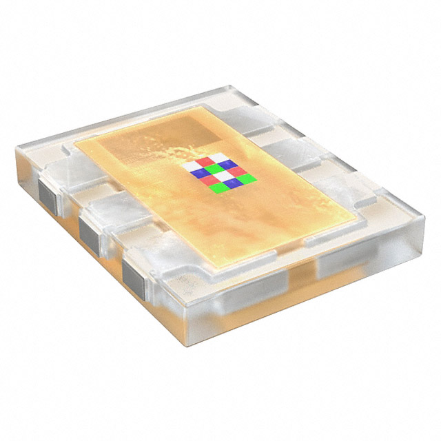
I/O Pins Confi guration
PIN NAME TYPE DESCRIPTION
1 SDA I/O I 2 C serial data I/O terminal – serial data I/O for I 2 C.
2 INT O Interrupt – open drain.
3 LDR  I LED driver for proximity emitter – up to 100 mA, open drain.
4 LEDK O LED Cathode, connect to LDR pin in most systems to use internal LED driver circuit
5 LEDA I LED Anode, connect to V BATT on PCB
6 GND Power supply ground. All voltages are referenced to GND.
7 SCL I I 2 C serial clock input terminal – clock ** for I 2 C serial data.
8 V DD Power Supply voltage.
Absolute Maximum Ratings over operating free-air temperature range (unless otherwise noted) ?
Parameter Symbol Min Max Units Test Conditions
Power Supply voltage V DD 3.8 V
[1]
Digital voltage range -0.5 3.8 V
Digital output current I O -1 20 mA
Storage temperature range Tstg -40 85 °C
?
Stresses beyond those listed under “absolute maximum ratings” may cause permanent damage to the device. These are stress ratings only and
functional operation of the device at these or any other conditions beyond those indicated under “recommended operating conditions” is not
implied. Exposure to absolute-maximum-rated conditions for extended periods may aff ect device reliability.
Note:
1. All voltages are with respect to GND.
Recommended Operating Conditions
Parameter Symbol Min Typ Max Units
Operating Ambient Temperature T A -30 85 °C
Supply voltage V DD 2.2 3.0 3.6 V
Supply Voltage Accuracy, V DD
total error including transients
-3 +3 %
LED Supply Voltage V BATT 2.5 4.5 V